- 您现在的位置:买卖IC网 > Sheet目录3841 > PIC16F737-I/SP (Microchip Technology)IC PIC MCU FLASH 4KX14 28DIP
PIC16F7X7
DS30498C-page 12
2004 Microchip Technology Inc.
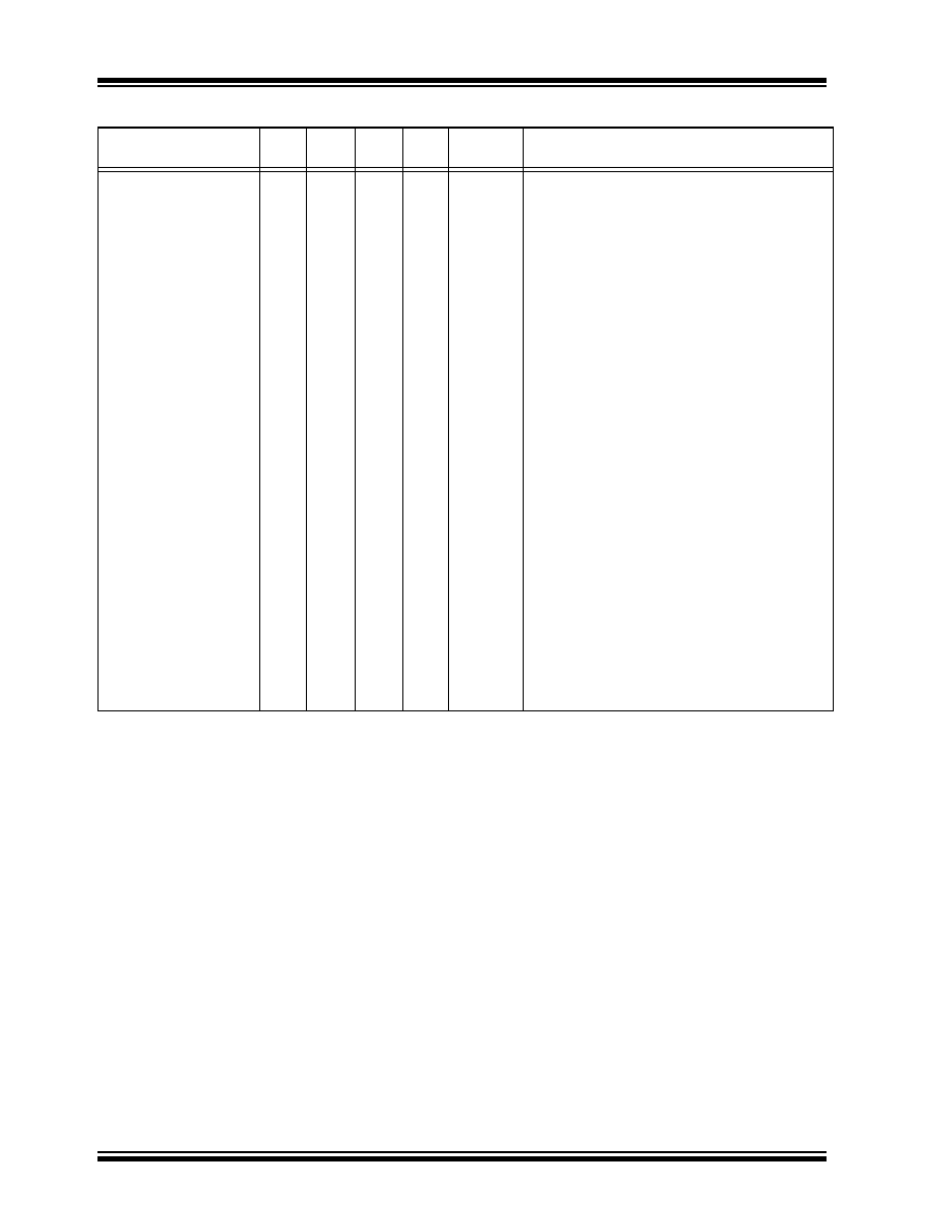
PORTB is a bidirectional I/O port. PORTB can be
software programmed for internal weak pull-up on all
inputs.
RB0/INT/AN12
RB0
INT
AN12
33
9
8
I/O
I
TTL/ST(1)
Digital I/O.
External interrupt.
Analog input channel 12.
RB1/AN10
RB1
AN10
34
10
9
I/O
I
TTL
Digital I/O.
Analog input channel 10.
RB2/AN8
RB2
AN8
35
11
10
I/O
I
TTL
Digital I/O.
Analog input channel 8.
RB3/CCP2/AN9
RB3
CCP2(5)
AN9
36
12
11
I/O
I
TTL
Digital I/O.
CCP2 capture input, compare output, PWM output.
Analog input channel 9.
RB4/AN11
RB4
AN11
37
14
I/O
I
TTL
Digital I/O.
Analog input channel 11
RB5/AN13/CCP3
RB5
AN13
CCP3
38
15
I/O
I
TTL
Digital I/O.
Analog input channel 13.
CCP3 capture input, compare output, PWM output.
RB6/PGC
RB6
PGC
39
16
I/O
TTL/ST(2)
Digital I/O.
In-Circuit Debugger and ICSP programming
clock.
RB7/PGD
RB7
PGD
40
17
I/O
TTL/ST(2)
Digital I/O.
In-Circuit Debugger and ICSP programming
data.
TABLE 1-3:
PIC16F747 AND PIC16F777 PINOUT DESCRIPTION (CONTINUED)
Pin Name
PDIP
Pin #
QFN
Pin #
TQFP
Pin #
I/O/P
Type
Buffer
Type
Description
Legend:
I = input
O = output
I/O = input/output
P = power
— = Not used
TTL = TTL input
ST = Schmitt Trigger input
Note
1:
This buffer is a Schmitt Trigger input when configured as an external interrupt.
2:
This buffer is a Schmitt Trigger input when used in Serial Programming mode.
3:
This buffer is a Schmitt Trigger input when configured as a general purpose I/O and a TTL input when used in the Parallel
Slave Port mode (for interfacing to a microprocessor bus).
4:
This buffer is a Schmitt Trigger input when configured in RC Oscillator mode and a CMOS input otherwise.
5:
Pin location of CCP2 is determined by the CCPMX bit in Configuration Word Register 1.
发布紧急采购,3分钟左右您将得到回复。
相关PDF资料
PIC18F86K22-I/PTRSL
MCU PIC 64K FLASH XLP 80TQFP
PIC16C63A-04I/SP
IC MCU OTP 4KX14 PWM 28DIP
PIC16C63A-04I/SO
IC MCU OTP 4KX14 PWM 28SOIC
52559-2270
CONN FFC 22POS .5MM VERT ZIF SMD
52559-1870
CONN FFC 18POS .5MM VERT ZIF SMD
DSPIC33EP64MC506-I/PT
IC DSC 16BIT 64KB FLASH 64TQFP
52745-1896
CONN FFC 18POS .5MM R/A ZIF SMD
PIC16LC622-04/P
IC MCU OTP 2KX14 COMP 18DIP
相关代理商/技术参数
PIC16F737-I/SP
制造商:Microchip Technology Inc 功能描述:IC 8BIT FLASH MCU 16F737 SDIL28
PIC16F737-I/SS
功能描述:8位微控制器 -MCU 7KB 368 RAM 25 I/O RoHS:否 制造商:Silicon Labs 核心:8051 处理器系列:C8051F39x 数据总线宽度:8 bit 最大时钟频率:50 MHz 程序存储器大小:16 KB 数据 RAM 大小:1 KB 片上 ADC:Yes 工作电源电压:1.8 V to 3.6 V 工作温度范围:- 40 C to + 105 C 封装 / 箱体:QFN-20 安装风格:SMD/SMT
PIC16F737T-I/ML
功能描述:8位微控制器 -MCU 7KB 368 RAM 25 I/O RoHS:否 制造商:Silicon Labs 核心:8051 处理器系列:C8051F39x 数据总线宽度:8 bit 最大时钟频率:50 MHz 程序存储器大小:16 KB 数据 RAM 大小:1 KB 片上 ADC:Yes 工作电源电压:1.8 V to 3.6 V 工作温度范围:- 40 C to + 105 C 封装 / 箱体:QFN-20 安装风格:SMD/SMT
PIC16F737T-I/SO
功能描述:8位微控制器 -MCU 7KB 368 RAM 25 I/O RoHS:否 制造商:Silicon Labs 核心:8051 处理器系列:C8051F39x 数据总线宽度:8 bit 最大时钟频率:50 MHz 程序存储器大小:16 KB 数据 RAM 大小:1 KB 片上 ADC:Yes 工作电源电压:1.8 V to 3.6 V 工作温度范围:- 40 C to + 105 C 封装 / 箱体:QFN-20 安装风格:SMD/SMT
PIC16F737T-I/SS
功能描述:8位微控制器 -MCU 7KB 368 RAM 25 I/O RoHS:否 制造商:Silicon Labs 核心:8051 处理器系列:C8051F39x 数据总线宽度:8 bit 最大时钟频率:50 MHz 程序存储器大小:16 KB 数据 RAM 大小:1 KB 片上 ADC:Yes 工作电源电压:1.8 V to 3.6 V 工作温度范围:- 40 C to + 105 C 封装 / 箱体:QFN-20 安装风格:SMD/SMT
PIC16F73-E/ML
功能描述:8位微控制器 -MCU 7 KB 368 RAM 25I/O RoHS:否 制造商:Silicon Labs 核心:8051 处理器系列:C8051F39x 数据总线宽度:8 bit 最大时钟频率:50 MHz 程序存储器大小:16 KB 数据 RAM 大小:1 KB 片上 ADC:Yes 工作电源电压:1.8 V to 3.6 V 工作温度范围:- 40 C to + 105 C 封装 / 箱体:QFN-20 安装风格:SMD/SMT
PIC16F73-E/SO
功能描述:8位微控制器 -MCU 7KB 192 RAM 22 I/O RoHS:否 制造商:Silicon Labs 核心:8051 处理器系列:C8051F39x 数据总线宽度:8 bit 最大时钟频率:50 MHz 程序存储器大小:16 KB 数据 RAM 大小:1 KB 片上 ADC:Yes 工作电源电压:1.8 V to 3.6 V 工作温度范围:- 40 C to + 105 C 封装 / 箱体:QFN-20 安装风格:SMD/SMT
PIC16F73-E/SP
功能描述:8位微控制器 -MCU 7KB 192 RAM 22 I/O RoHS:否 制造商:Silicon Labs 核心:8051 处理器系列:C8051F39x 数据总线宽度:8 bit 最大时钟频率:50 MHz 程序存储器大小:16 KB 数据 RAM 大小:1 KB 片上 ADC:Yes 工作电源电压:1.8 V to 3.6 V 工作温度范围:- 40 C to + 105 C 封装 / 箱体:QFN-20 安装风格:SMD/SMT